
Introduction
For more than ten years, physicists knew a topological crystalline insulator should exist. They just couldn’t build it.
Now they have. Researchers in Finland have successfully created a two-dimensional topological crystalline insulator, a quantum material scientists first predicted over a decade ago but could never physically produce. The breakthrough could bring room-temperature quantum electronics much closer to reality.
This isn’t just an academic milestone. This discovery matters because it opens the door to faster, more efficient electronics that don’t require the extreme cold most quantum devices depend on. If you’ve ever wondered why quantum computers live in refrigerator-sized cooling systems, this research points toward a future where that might not be necessary electronics.
What Exactly Did Scientists Build?
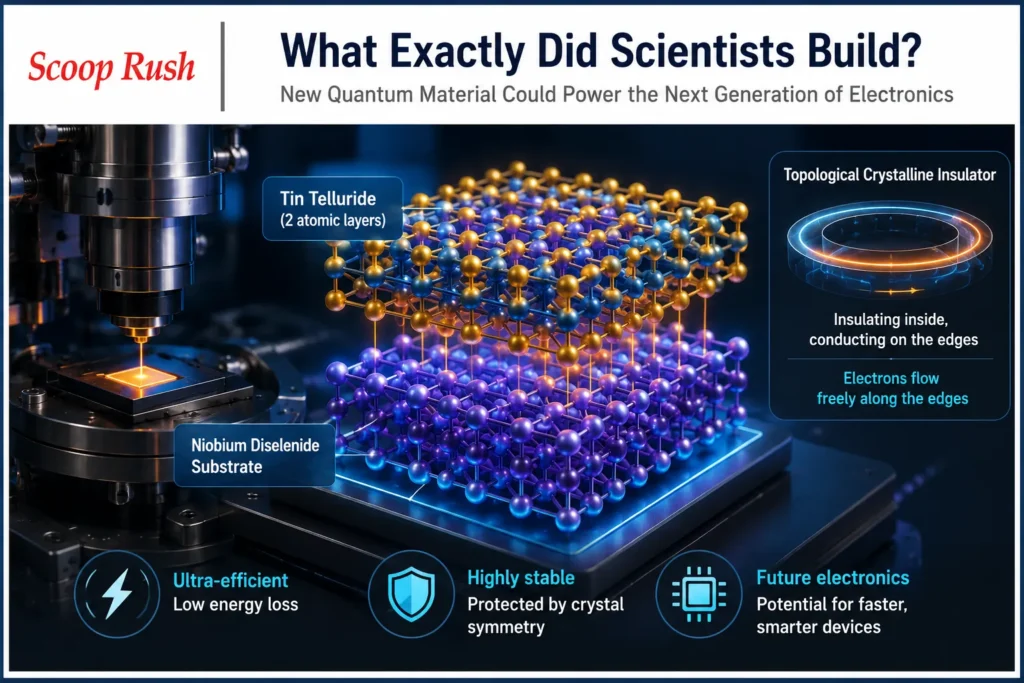
Physicists from the University of Jyväskylä and Aalto University in Finland created the material by growing an ultra-thin film made of just two layers of tin telluride. They placed this film on top of a niobium diselenide substrate, essentially stacking two different quantum materials to create something entirely new.
The team was led by Associate Professor Kezilbeiek Shawulienu, working alongside Aalto University researchers Professor Peter Liljeroth and Professor Jose Lado. Their combined expertise made it possible to finally overcome a problem that had stumped scientists for years: finding the right materials and conditions to actually build this theoretical structure.
Until now, every attempt to create this material had run into the same wall. The right combination of materials simply didn’t exist, or couldn’t be manufactured with enough precision.
Why This Material Is So Special
Topological crystalline insulators sound complicated, but the core idea is fairly simple. These materials act as insulators on the inside, meaning electricity doesn’t flow through their bulk. However, their edges behave completely differently.
Along the edges, electrons can travel freely through special conducting pathways. These pathways are protected by the symmetry of the material’s crystal structure, which means they’re remarkably stable and resistant to disruption.
This property makes topological materials incredibly valuable for electronics. Engineers could potentially use these edge states to move information with minimal energy loss, something conventional materials struggle to achieve.
How Researchers Confirmed the Discovery
Building the material was only half the challenge. The team needed to prove it actually behaved the way theory predicted.
To do this, researchers used molecular beam epitaxy combined with low-temperature scanning tunneling microscopy. This approach allowed them to examine the material’s electronic behavior at the atomic level, essentially watching individual atoms and their surrounding electron activity.
Their measurements revealed exactly what they were hoping to find: pairs of conducting edge states running along the material’s boundaries. This is the defining signature of a topological crystalline insulator, and its presence confirmed the material worked as predicted.
The Role of Strain in Stabilizing the Material
Here’s where things get particularly interesting. The researchers discovered that the tin telluride film gets compressed by the niobium diselenide substrate underneath it. This compression creates strain within the material.
That strain isn’t a flaw. It’s essential. Without it, the topological state wouldn’t stabilize at all.
Even more importantly, the team found they could adjust the edge states simply by changing the amount of strain applied to the material. This gives scientists a practical, controllable way to fine-tune the material’s electronic properties, something that could prove extremely valuable for future device engineering.
The conducting edge states also appear within a large electronic band gap, measuring more than 0.2 electron volts. This gap size matters because it directly relates to how stable the material remains under different conditions.
Why Room-Temperature Quantum Electronics Would Be a Big Deal
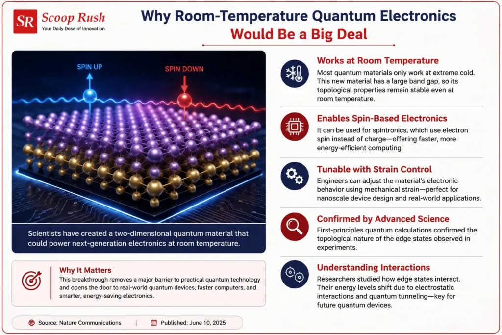
Most quantum materials only display their special properties at extremely low temperatures, often colder than outer space. This requirement makes quantum devices expensive, bulky, and impractical for everyday use.
Because this newly created material has a relatively large band gap, researchers expect its topological properties to remain stable even at room temperature. Therefore, this discovery could eliminate one of the biggest barriers standing between quantum technology and real-world application.
Consequently, this material could serve as a foundation for spin-based electronics, which use the magnetic spin of electrons rather than just their charge to process and store information. Spintronic devices are widely seen as a promising path toward faster, more energy-efficient computing.
Additionally, the material’s tunable nature through strain control makes it especially attractive for nanoscale device design. Engineers could potentially adjust a device’s electronic behavior after manufacturing, simply by controlling mechanical strain rather than redesigning the entire structure.
The Science Behind the Confirmation
The Finnish research team didn’t stop at experimental observation. They also ran first-principles quantum mechanical calculations to verify that the edge states they observed truly had a topological origin, rather than resulting from some other electronic effect.
These calculations confirmed the experimental findings, giving the research added scientific weight. The team also studied how neighboring edge states interact with one another. They found that the energy levels of these states shift because of a combination of electrostatic interactions and quantum tunneling.
Understanding these interactions matters because future devices will likely need multiple edge states working together. Knowing how they influence each other is a necessary step toward designing functional quantum electronics.
The full findings were published in the journal Nature Communications, a peer-reviewed publication known for high-impact scientific research.
What This Means for the Future of Electronics

While practical, room-temperature quantum devices aren’t arriving tomorrow, this discovery represents a meaningful step forward. Scientists have spent over a decade trying to physically realize this material, and now that goal has been achieved.
Moreover, the ability to control edge states through strain offers researchers a tunable, practical method for future experimentation. This flexibility could accelerate progress in fields ranging from quantum computing to advanced nanoscale sensors.
As a result, this research adds Finland to the growing list of countries pushing the boundaries of quantum material science. Similarly, it strengthens the broader global effort to make quantum technology more accessible and less dependent on extreme cooling systems, much like ongoing efforts to understand ancient discoveries that reshape our understanding of the natural world.
Conclusion
Physicists have finally built a two-dimensional topological crystalline insulator, a material predicted more than ten years ago but never before achieved in the lab. By layering tin telluride on a niobium diselenide substrate, researchers created a material with protected conducting edge states and a large electronic band gap.
The discovery that strain can control these edge states gives scientists a practical tool for tuning the material’s properties. Because the band gap is large enough to remain stable at room temperature, this breakthrough brings practical quantum electronics significantly closer to reality.
Ultimately, this research offers real promise for spin-based electronics and next-generation nanoscale devices. While there’s still work ahead before these materials appear in consumer technology, this milestone marks meaningful progress toward that future.
FAQs
Q1: What is a two-dimensional topological crystalline insulator?
A: It’s a quantum material that insulates electricity through its interior but allows electrons to flow freely along protected pathways at its edges. These edge states are stabilized by the material’s crystal symmetry.
Q2: Why did it take over a decade to create this material?
A: Scientists lacked the right combination of materials and manufacturing techniques needed to physically produce it. The breakthrough came from layering tin telluride on a niobium diselenide substrate, which created the necessary strain conditions.
Q3: How does strain affect the material’s quantum properties?
A: Strain from the underlying substrate compresses the tin telluride film, which stabilizes its topological state. Researchers also found that adjusting the strain lets them tune the material’s edge states, offering a controllable way to modify its behavior.
Q4: Could this material lead to room-temperature quantum computers?
A: It’s a promising step in that direction. Because the material’s band gap is large, its topological properties are expected to remain stable at room temperature, unlike many quantum materials that only work at extremely low temperatures.
Q5: Where was this research published?
A: The findings were published in Nature Communications, following research conducted by physicists at the University of Jyväskylä and Aalto University in Finland.

